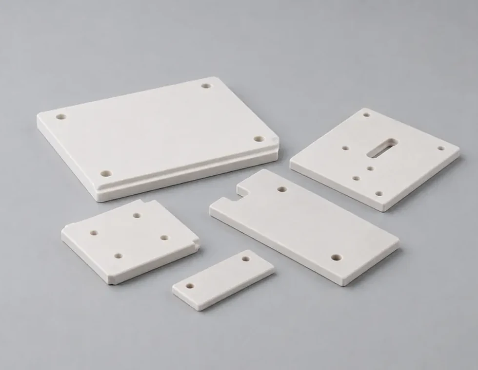
Flat Ceramic Structures
Ceramic Plates & Insulating Panels
Used where flatness, stability and insulating performance support chamber assemblies, carriers, supports or process fixtures.
Semiconductor ceramic components for vacuum, plasma, thermal and precision process equipment. These parts are used where dimensional stability, electrical insulation, cleanliness and process compatibility directly affect tool performance and product consistency.
Semiconductor ceramic components are usually selected around contamination control, stable electrical behavior, process compatibility and repeatable geometry inside complex equipment.
Components used in sensitive process equipment should support clean operation and help reduce avoidable contamination risk.
Ceramics are widely used where chambers, supports, feedthrough regions or fixtures require stable electrical separation.
Parts must remain dimensionally and functionally stable in equipment exposed to vacuum, thermal cycling or plasma-facing environments.
Controlled geometry supports repeatable assembly, stable wafer handling and predictable performance across production tools.
Semiconductor applications often use plates, discs, insulators, positioning parts and custom ceramic interfaces shaped around chamber layout, wafer path and electrical design.
Used where flatness, stability and insulating performance support chamber assemblies, carriers, supports or process fixtures.
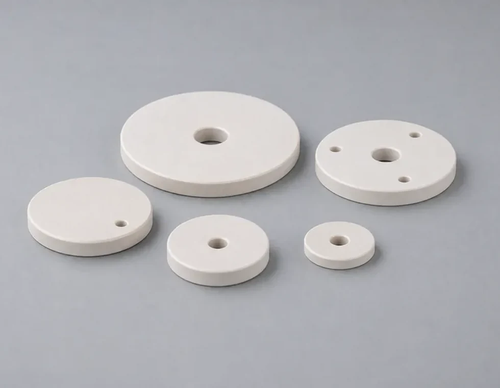
Applied where concentricity, face quality and stable geometry are important for chamber interfaces, support structures or process positioning.
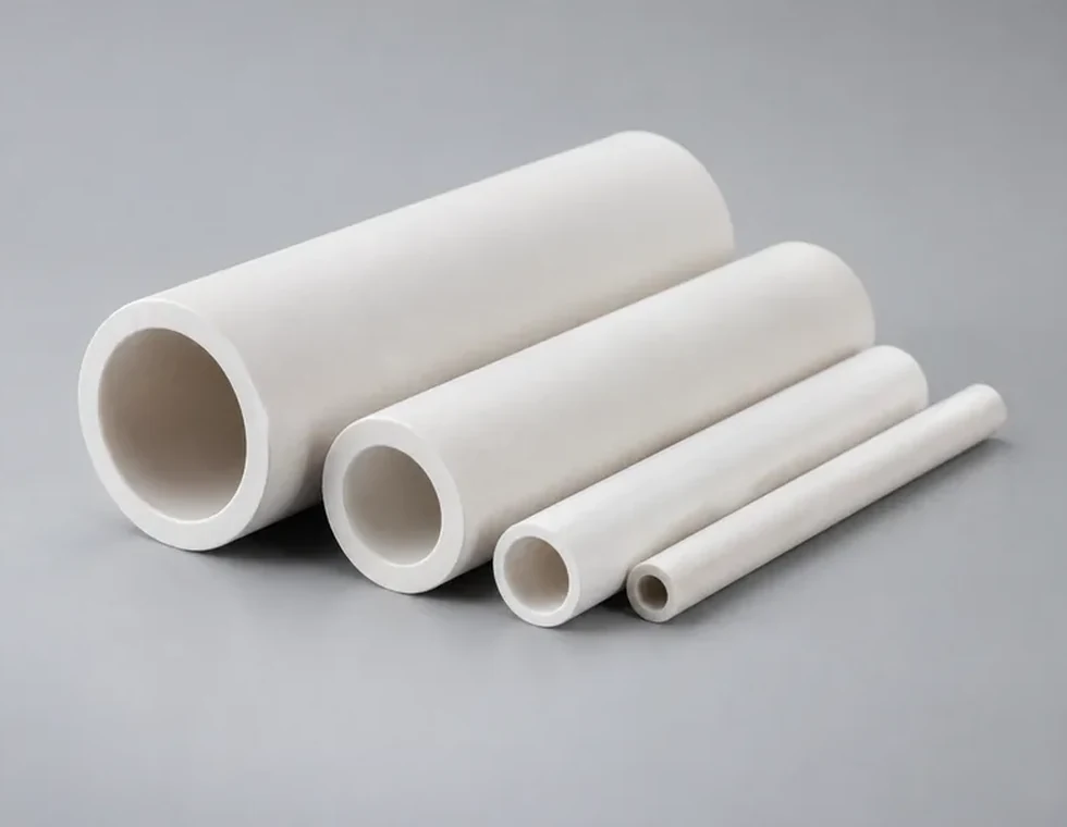
Used to isolate conductors, guide assemblies or support electrical interfaces inside semiconductor equipment.
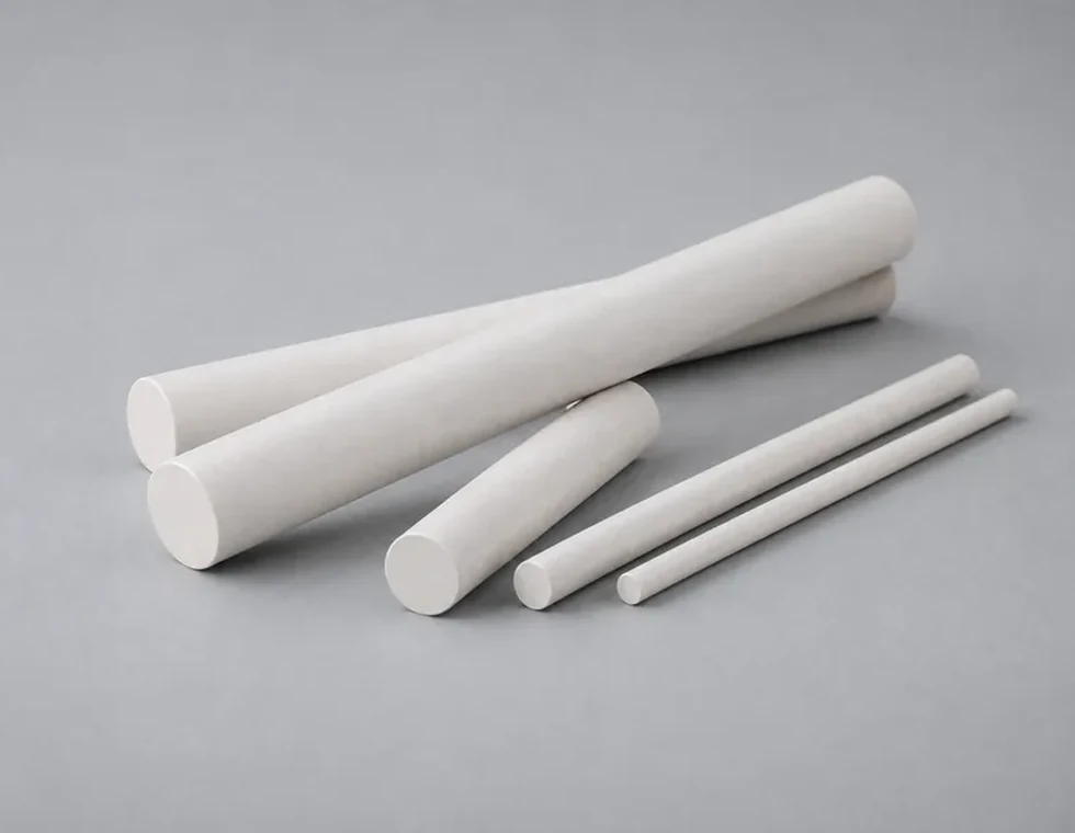
Precision ceramic components for alignment, support, movement control and fixture stability in process or handling assemblies.
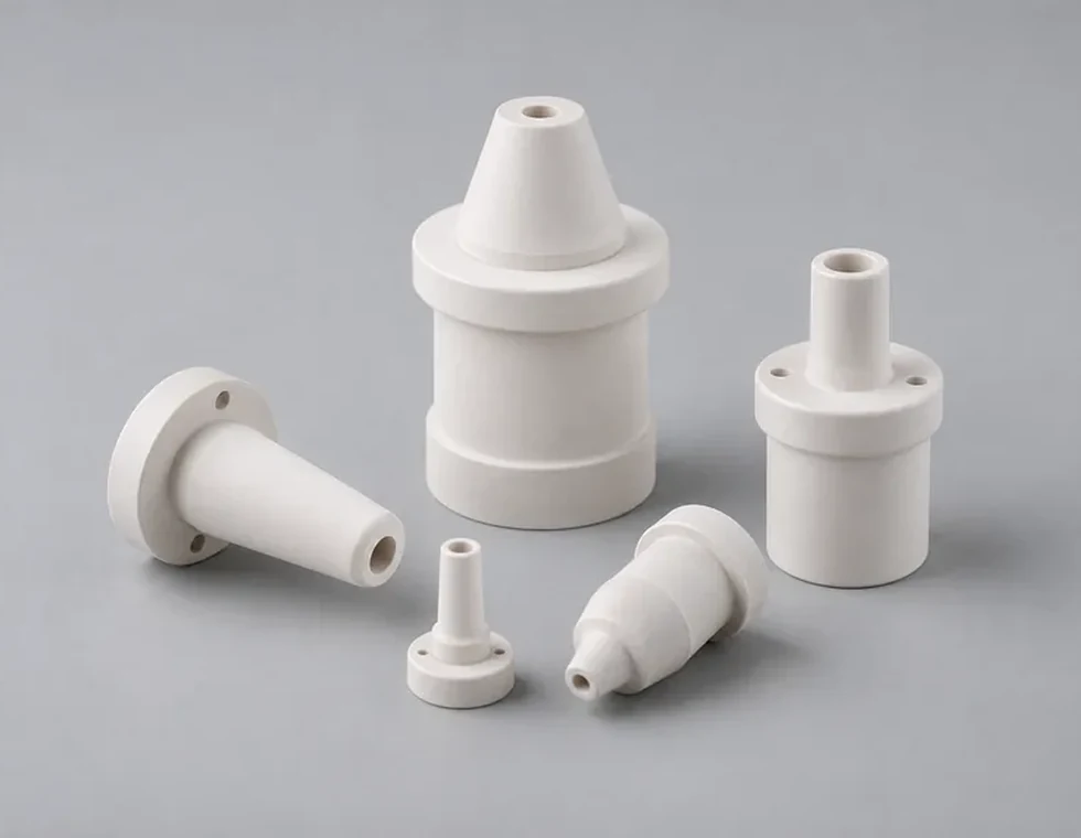
Flow-related ceramic components used where chemical stability, wear resistance and controlled geometry are important to the process path.
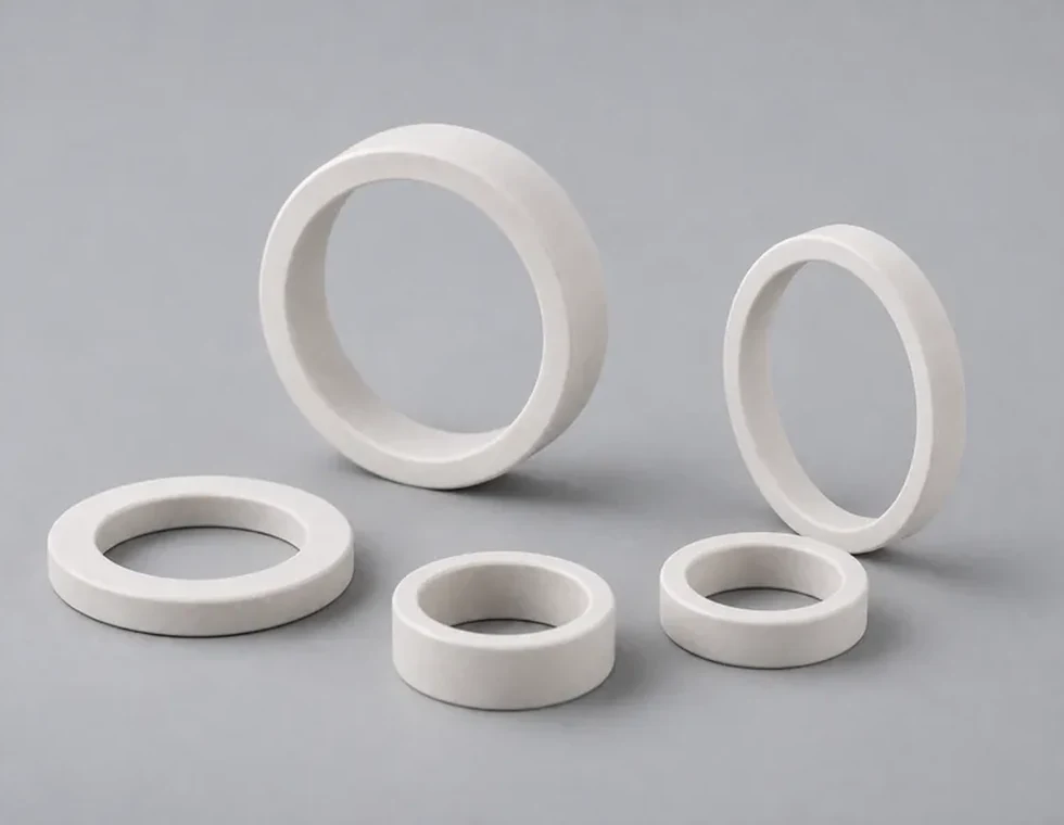
Drawing-based ceramic parts tailored to the chamber, fixture, feedthrough, support or handling requirements of specialized semiconductor tools.
Semiconductor ceramic components should be reviewed around the actual equipment environment. A part that is dimensionally correct on paper may still underperform if process exposure, assembly datums or cleanliness requirements are not considered.
Vacuum level, plasma exposure, temperature and process chemistry all influence the most suitable ceramic solution.
Flatness, concentricity, thickness and feature location should support accurate assembly and stable equipment performance.
Edges, contact surfaces and moving interfaces should be reviewed carefully where the application is sensitive to wear debris or handling damage.
Insulation path, mounting geometry and interface design should be aligned with the electrical demands of the specific semiconductor tool.
Semiconductor components often combine simple shapes with tight control on only a few critical dimensions. This keeps the part manufacturable while preserving the geometry that truly matters in equipment assembly.
Material selection should balance dielectric behavior, thermal performance, purity, dimensional stability and compatibility with the specific process area of the equipment.
A widely used ceramic for semiconductor equipment where electrical insulation, dimensional stability and broad industrial applicability are important.
Relevant where thermal management and ceramic performance need to be considered together in demanding equipment designs.
Useful where higher toughness or resistance to local mechanical damage helps support the function of a precision component.
Other ceramics can be evaluated when the application places stronger emphasis on purity, dielectric behavior or process-specific compatibility.
Most semiconductor equipment problems linked to ceramics come from interface details, handling points or process mismatch—not from the material name alone.
Edges, wear surfaces and repeated contact zones should be reviewed carefully where particle control is important to the process.
Even stable ceramics can create system-level issues if mating parts, clamping methods or thermal gradients are not considered together.
A part may need different geometry or material depending on whether it works near plasma, vacuum interfaces, heated zones or wet-process equipment.
Semiconductor ceramic components are used where equipment reliability depends on clean insulating structures, stable geometry and precise process interfaces.
Ceramic parts used in or around chamber structures where isolation, stability and process compatibility are required.
Components developed for electrically and dimensionally sensitive environments associated with plasma-based processing hardware.
Ceramic supports, spacers and positioning parts used where precise geometry helps stabilize handling and placement.
Parts used to isolate conductors, mount assemblies or create stable electrical boundaries inside complex tools.
Ceramics used in equipment where dimensional stability and insulating performance must remain consistent at elevated temperature.
Drawing-based ceramic components tailored to equipment manufacturers building specialized semiconductor process systems.
Semiconductor ceramic inspection should focus on the dimensions, surfaces and visible edge quality that influence alignment, contact behavior and the final equipment interface.
The most useful RFQs explain where the ceramic sits in the equipment and what it needs to do there. That context helps determine material, tolerances, edge treatment and the most important inspection points.
They are used in semiconductor equipment where electrical insulation, process compatibility, dimensional stability and clean operation are important to the tool design.
Yes. Drawing-based ceramic components can be evaluated according to geometry, material, functional surfaces, process exposure and expected production volume.
Because the same geometry may require different material choices or edge, surface and tolerance strategies depending on whether the part is used in vacuum, plasma, thermal or other process zones.
Yes. Features such as holes, slots, steps, rings, bores and precision surfaces can be reviewed according to the functional needs of the equipment and the selected ceramic material.
Please provide the drawing, material preference, critical dimensions, process location, operating environment, functional requirements and expected quantities.
Send your drawing and process conditions for an engineering review focused on precision, cleanliness and tool compatibility.